- 您现在的位置:买卖IC网 > Sheet目录3822 > PIC16F77-I/L (Microchip Technology)IC MCU FLASH 8KX14 A/D 44PLCC
2002 Microchip Technology Inc.
DS30325B-page 29
PIC16F7X
3.0
READING PROGRAM MEMORY
The FLASH Program Memory is readable during nor-
mal operation over the entire VDD range. It is indirectly
addressed through Special Function Registers (SFR).
Up to 14-bit numbers can be stored in memory for use
as calibration parameters, serial numbers, packed 7-bit
ASCII, etc. Executing a program memory location con-
taining data that forms an invalid instruction results in a
NOP
.
There are five SFRs used to read the program and
memory. These registers are:
PMCON1
PMDATA
PMDATH
PMADR
PMADRH
The program memory allows word reads. Program
memory access allows for checksum calculation and
reading calibration tables.
When interfacing to the program memory block, the
PMDATH:PMDATA registers form a two-byte word,
which
holds
the
14-bit
data
for
reads.
The
PMADRH:PMADR registers form a two-byte word,
which holds the 13-bit address of the FLASH location
being accessed. These devices can have up to 8K
words of program FLASH, with an address range from
0h to 3FFFh. The unused upper bits in both the
PMDATH and PMADRH registers are not implemented
and read as “0’s”.
3.1
PMADR
The address registers can address up to a maximum of
8K words of program FLASH.
When selecting a program address value, the MSByte
of the address is written to the PMADRH register and
the LSByte is written to the PMADR register. The upper
MSbits of PMADRH must always be clear.
3.2
PMCON1 Register
PMCON1 is the control register for memory accesses.
The control bit RD initiates read operations. This bit
cannot be cleared, only set, in software. It is cleared in
hardware at the completion of the read operation.
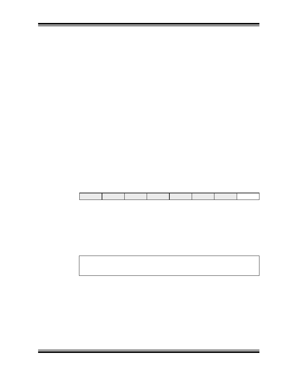
REGISTER 3-1:
PMCON1 REGISTER (ADDRESS 18Ch)
R-1
U-0
U-x
U-0
R/S-0
reserved
—
RD
bit 7
bit 0
bit 7
Reserved: Read as ‘1’
bit 6-1
Unimplemented: Read as '0'
bit 0
RD: Read Control bit
1
= Initiates a FLASH read, RD is cleared in hardware. The RD bit can only be set (not cleared)
in software.
0
= FLASH read completed
Legend:
R = Readable bit
W = Writable bit
U = Unimplemented bit, read as ‘0’
- n = Value at POR reset
’1’ = Bit is set
’0’ = Bit is cleared
x = Bit is unknown
发布紧急采购,3分钟左右您将得到回复。
相关PDF资料
PIC18F4525-I/ML
IC MCU FLASH 24KX16 44QFN
DSPIC30F2023-30I/ML
IC DSPIC MCU/DSP 12K 44QFN
PIC16LF767-I/ML
IC PIC MCU FLASH 8KX14 28QFN
PIC18LF2320-I/SO
IC MCU FLASH 4KX16 EEPROM 28SOIC
PIC18F4458-I/ML
IC PIC MCU FLASH 12KX16 44QFN
DSPIC33FJ64GP706A-I/PT
IC DSPIC MCU/DSP 64K 64-TQFP
PIC16F874-20/P
IC MCU FLASH 4KX14 EE 40DIP
DSPIC33FJ64GP706-I/PT
IC DSPIC MCU/DSP 64K 64TQFP
相关代理商/技术参数
PIC16F77-I/L
制造商:Microchip Technology Inc 功能描述:8BIT FLASH MCU SMD 16F77 PLCC44
PIC16F77-I/ML
功能描述:8位微控制器 -MCU 14KB 368 RAM 33 I/O RoHS:否 制造商:Silicon Labs 核心:8051 处理器系列:C8051F39x 数据总线宽度:8 bit 最大时钟频率:50 MHz 程序存储器大小:16 KB 数据 RAM 大小:1 KB 片上 ADC:Yes 工作电源电压:1.8 V to 3.6 V 工作温度范围:- 40 C to + 105 C 封装 / 箱体:QFN-20 安装风格:SMD/SMT
PIC16F77-I/P
功能描述:8位微控制器 -MCU 14KB 368 RAM 33 I/O RoHS:否 制造商:Silicon Labs 核心:8051 处理器系列:C8051F39x 数据总线宽度:8 bit 最大时钟频率:50 MHz 程序存储器大小:16 KB 数据 RAM 大小:1 KB 片上 ADC:Yes 工作电源电压:1.8 V to 3.6 V 工作温度范围:- 40 C to + 105 C 封装 / 箱体:QFN-20 安装风格:SMD/SMT
PIC16F77-I/P
制造商:Microchip Technology Inc 功能描述:IC 8BIT FLASH MCU 16F77 DIP40
PIC16F77-I/PG
功能描述:8位微控制器 -MCU 14KB 368 RAM 33 I/O RoHS:否 制造商:Silicon Labs 核心:8051 处理器系列:C8051F39x 数据总线宽度:8 bit 最大时钟频率:50 MHz 程序存储器大小:16 KB 数据 RAM 大小:1 KB 片上 ADC:Yes 工作电源电压:1.8 V to 3.6 V 工作温度范围:- 40 C to + 105 C 封装 / 箱体:QFN-20 安装风格:SMD/SMT
PIC16F77-I/PT
功能描述:8位微控制器 -MCU 14KB 368 RAM 33 I/O RoHS:否 制造商:Silicon Labs 核心:8051 处理器系列:C8051F39x 数据总线宽度:8 bit 最大时钟频率:50 MHz 程序存储器大小:16 KB 数据 RAM 大小:1 KB 片上 ADC:Yes 工作电源电压:1.8 V to 3.6 V 工作温度范围:- 40 C to + 105 C 封装 / 箱体:QFN-20 安装风格:SMD/SMT
PIC16F77-I/PT
制造商:Microchip Technology Inc 功能描述:8BIT FLASH MCU SMD 16F77 TQFP44
PIC16F77-I/PTG
功能描述:8位微控制器 -MCU 14KB 368 RAM 33 I/O RoHS:否 制造商:Silicon Labs 核心:8051 处理器系列:C8051F39x 数据总线宽度:8 bit 最大时钟频率:50 MHz 程序存储器大小:16 KB 数据 RAM 大小:1 KB 片上 ADC:Yes 工作电源电压:1.8 V to 3.6 V 工作温度范围:- 40 C to + 105 C 封装 / 箱体:QFN-20 安装风格:SMD/SMT